Your Cart is Empty
16011
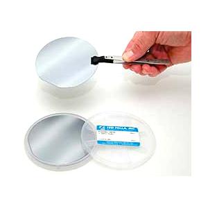
These 1", 2", 3", 4" and 6" diameter silicon wafers can be used either as a substrate for thin film research or to make small silicon substrates by dicing the wafer into smaller pieces using a scriber and the Wafer Cleaving / Glass Breaking Pliers. The wafer is shipped in a wafer carrier.
Wafer Mounting Film
Properties:
16011 - Ø1" Silicon Wafer, Type P / <100>
16012 - Ø2" Silicon Wafer, Type P / <100>
16013 - Ø3" Silicon Wafer, Type P / <111>
16010 - Ø4" Silicon Wafer, Type P / <100>
16015 - Ø6" Silicon Wafer, Type P / <100>